
Researchers at Utrecht University gain control over growth 2D material
Researchers all over the world have been diving into 2D materials such as graphene, because these materials allow to generate a multitude of material properties using only very little material. Graphene is actually not the most useful 2D material, because it is a metal.
In order to replace conventional computer chips with energy-saving 2D computer chips, for example, so-called semiconductors are needed. The 2D material tungsten disulphide (WS2) is only 3 atoms thick and is a promising candidate as a 2D semiconductor. In addition to applications in electronics, the material is also suitable for promoting chemical reactions (catalysis), which means that less energy is needed in chemical factories.

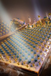
At Utrecht University, scientists Marijn van Huis and Dnyaneshwar Gavhane have now witnessed the growth process of this 2D material live inside the electron microscope (EM) by heating a solution from which the 2D material can grow. If they heat a thin layer of growth solution, the 2D material grows horizontally and when they heat a thick layer of growth solution, the 2D material grows vertically, with edges pointing upward. They can steer the growth to take place either horizontally or vertically. If in addition they cover the underground with gold or platina nanoparticles, the growth of the 2D material is much stronger and it becomes much larger. In addition, they discovered that when a metallic underground is used ‘twisted’ layers were formed, where two layers of WS2 are overlapping but in a twisted manner, which generates even more electric properties to the material. They have now published their research in the esteemed journal Advanced Functional Materials, including various videos showing the growth process.